Diagnose & scope
Clarify the problem, constraints and success criteria.
Schematic review, component selection, layout guidance, BOM preparation and prototype test planning.
Support for moving an electronics concept from breadboard or block diagram toward a manufacturable, testable PCB prototype.
We work through consultation, review, engineering guidance and knowledge transfer. For academic work, researcher ownership and responsibility remain explicit.
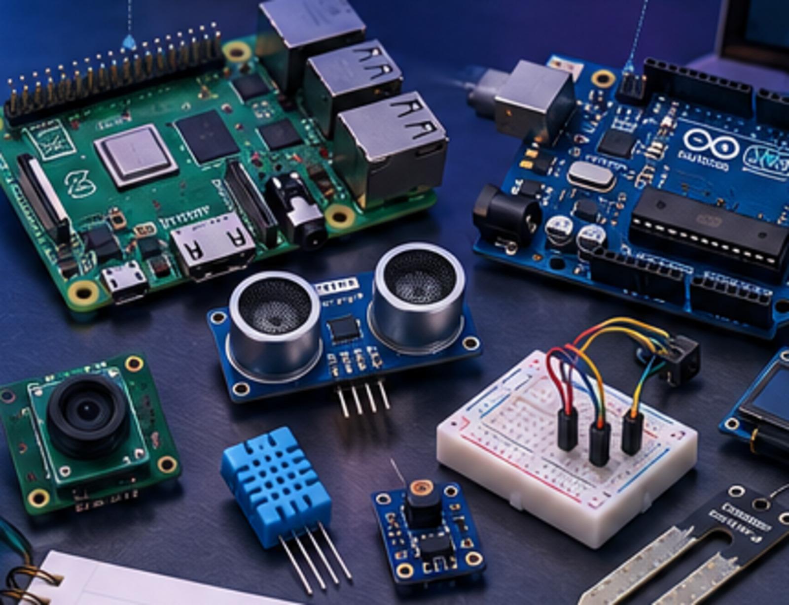
We support engineering builds with Raspberry Pi, Arduino, ESP32, sensors, measurement circuits and communication interfaces—paired with documented testing and reviewable results.
Details vary by project, but the control points stay consistent.
Clarify the problem, constraints and success criteria.
Choose tools and define milestones and outputs.
Incremental implementation with testing and review.
Documentation, explanation and next-step readiness.
Common workflows include KiCad, Altium-style design reviews and standard Gerber/BOM handoff practices.
Embedded-system architecture, firmware guidance, sensor integration and prototype validation.
Explore service hardwareConnected devices, sensing, MQTT/API communication, dashboards and remote monitoring architecture.
Explore service hardwareSensor selection, calibration, signal conditioning, control logic and end-to-end validation.
Explore service